
OVERVIEW
The TrueSilicon's AXI to APB Bridge is a high-performance protocol converter IP designed to enable seamless communication between AXI master devices and APB slave peripherals in modern System-on-Chip (SoC) architectures.
This bridge efficiently translates high-speed AXI transactions into APB protocol transfers, allowing processors, DMA controllers, and other AXIcompliant masters to access low-speed peripheral devices such as UARTs, timers, and configuration registers. With configurable data widths for both interfaces, flexible address width options, and support for both synchronous and asynchronous clock domain operation, the bridge offers the versatility required for diverse SoC designs.
The IP supports outstanding transactions, all AXI burst types, and unaligned address handling while maintaining minimal latency of just 2 clock cycles. It features comprehensive error detection with interrupt generation capabilities, ensuring robust operation and simplified system debugging.
The RTL is fully lint- clean and synthesis-ready, having undergone rigorous verification to meet industry-standard coding guidelines and best practices. Power efficiency is optimized through intelligent clock gating mechanisms and configurable clock enable/disable features, making it suitable for power-sensitive applications.
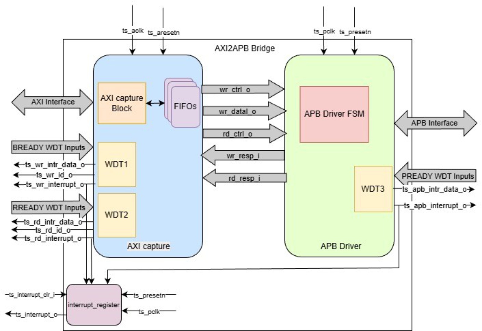
Figure -1 Bridge Architecture
Figure 1 shows the internal architecture of the AXI to APB bridge. The bridge mainly consists of two func onal blocks: the AXI Capture block and the APB Driver block, connected through control and data FIFOs. Overall the bridge delivers an opmal balance of performance, flexibility, power efficiency, and reliability for integra on into advanced semiconductor designs.
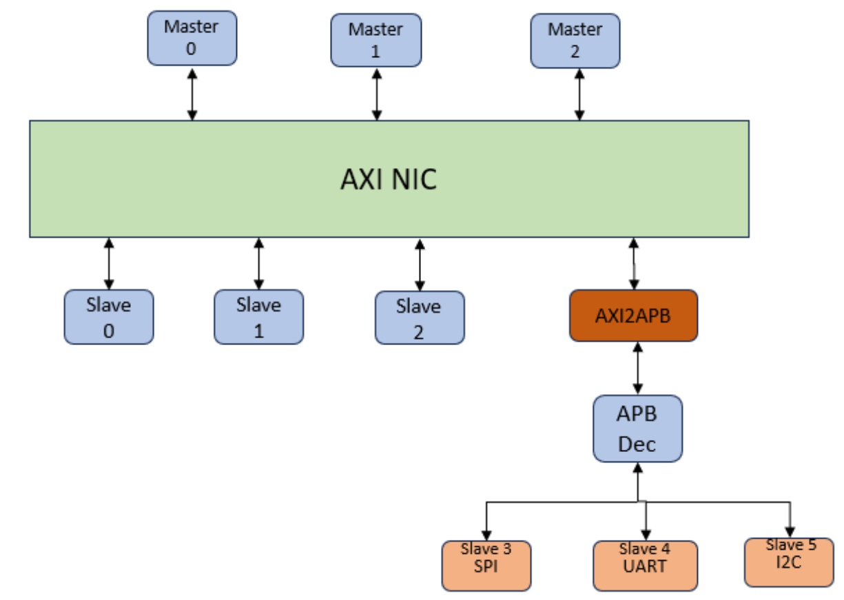
Figure -2 Bridge Connec on in NIC/SoC