The TrueSilicon DMA controller is a highly efficient hardware IP block designed to offload data movement operations from the processor to maximize overall system performance.The IP integrates seamlessly into AMBA-based systems using an APB (Advanced Peripheral Bus) interface for configuration and control register access, ensuring lightweight integration into microcontroller and SoC environments.
The DMA acts as an autonomous bridge, allowing massive amounts of data to travel directly between high-speed RAM and slower communication peripherals without any processor intervention.
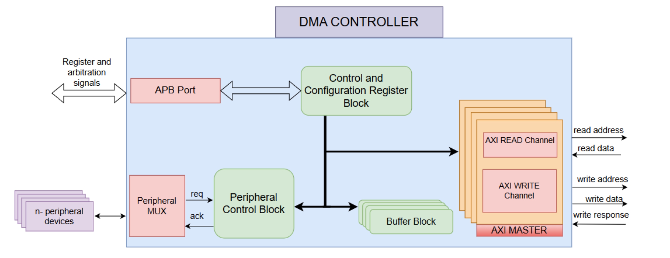
At the physical level, the hardware features a highly parameterized and scalable architecture. It can be configured with anywhere from 1 to 16 independent hardware channels. Each of these channels has its own dedicated FIFO buffer which prevents physical bus bottlenecks during concurrent transfers. To interface with the rest of the chip, the controller utilizes dual AXI4 Master Ports to carry the actual data payloads, and a single, narrow APB Slave Interface that the CPU uses to program the controller's internal registers.
The CPU initiates the transfer by configuring the DMA through the APB interface. After setting these parameters, the CPU enables the required DMA channel. Once triggered, the DMA takes over the data movement. The CPU then continues normal program execution without waiting for the transfer to complete.
After initialization, the DMA controller waits for a hardware trigger from an external peripheral. Peripherals like a UART or SPI controller have dedicated request lines. Request signal passes through a specialized peripheral multiplexer block inside the DMA, which maps up to 8 external hardware requests onto a single, designated internal DMA channel.
The DMA requests access to the shared system bus and waits for the arbiter to grant control. Once granted, it transfers data from source to destination using its AXI master interface, handling alignment and data formatting internally. After completing the transfer (based on the programmed size), it releases the bus and interrupts the CPU to indicate completion.
The fully synchronous RTL design ensures clean clock-domain operation, predictable timing behaviour, and straightforward static timing analysis (STA).
The architecture is optimized for power, performance, andarea (PPA),making it suitable for a wide range of technology nodes and applications.
Figure 1 depicts the high-level architecture of the TrueSiliconDMA Controller IP, including the APB driven control and configuration registers, multiple AXI Masters along with multiple buffers and multiple peripheral devices.