OVERVIEW
The TrueSilicon xSPI, standardized by JEDEC, is a high-performance serial interface designed primarily for non-volatile memory devices such as NOR flash. It extends traditional SPI by providing higher bandwidth, standardized communication, and flexible system integration, making it suitable for modern SoCs and embedded platforms.
At its core, xSPI supports both Single Data Rate (SDR) and Double Data Rate (DDR) transfers, operating up to 200MHz. In DDR mode, data is transferred on both clock edges, achieving an effective throughput of 400 MT/s, which is significantly higher than conventional SPI. To further enhance performance, xSPI enables parallel I/O with up to 8 data lines (Octal mode), allowing multiple bits to be transferred per clock cycle.
A single controller can communicate with multiple memory targets, each selected using a dedicated chip selectsignal. This simplifies system architecture while allowing multiple external memory devices to coexist efficiently.
From a physical interface perspective, xSPI defines 11 or 12 signal configurations, depending on whether an optional differential clock is used. Additionally, xSPI mandates a Power-On Reset (POR) to ensure the device initializes into a known safe state. It also provides optional features such as in-band reset commands and deep power-down modes to enhance control and reduce power consumption during idle periods.
To maintain backward compatibility, xSPI supports 1S-1S-1S mode, which mimics traditional single-bit SDR SPI operation for command, address, and data phases. For high-performance applications, it supports 8D-8D 8D mode, where command, address, and data phases all use 8-bit wide DDR transfers, enabling maximum throughput.
xSPI transactions are organized into clearly defined phases: Command, Command Modifier, Initial Latency, and Data. The command specifies the operation, while the command modifier allows flexible control over parameters such as data width, read/write behaviour, and protocol modes. The initial latency phase introduces programmable wait cycles to ensure the memory device is ready, followed by the data phase where actual data transfer occurs. This structured transaction model improves efficiency and ensures standardization across devices.
In addition to advanced features, xSPI retains support for a limited set of legacy SPI commands for basic identification and configuration. It also defines Command Profiles (1.0 and 2.0), which standardize command behavior and timing requirements, ensuring interoperability between different vendors' devices.
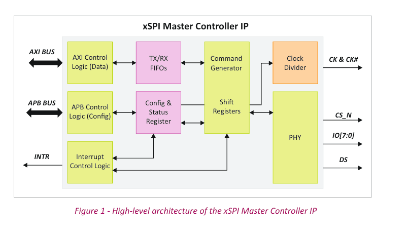
The controller configuration can be done through an APB interface and high-speed data access can be handled through an AXI interface. The APB side is usedto program internal control registers—such as operating mode (1S/8D, SDR/DDR), command profiles, latency cycles, and chip-select settings. Once configured, the AXI interface is used for actual memory transactions, where the external flash is mapped into the system address space. When the CPU or DMA issues an AXI read or write, the xSPI controller translates it into the appropriate command, address, latency, and data phases of the xSPI protocol, fetches or writes data to the flash at high speed, and returns it over AXI.
A key strength of xSPI lies in its flexibility. Through command modifiers and configuration settings, the controller can dynamically adjust read/write operations, latency cycles, and data bus width based on performance and system requirements. Furthermore, configurable latency cycles allow proper synchronization between the controller and memory device, which is critical for reliable operation at high speeds.