OVERVIEW
The TrueSilicon JTAG Controller IP is a standards-compliant test and debug interface designed to enable efficient boundary-scan testing, device configuration, and on-chip debugging in modern System-on-Chip (SoC) designs. Fully aligned with the IEEE 1149.1 specification, the controller provides a reliable mechanism for structural testing, fault isolation, and system-level debug access.
The IP implements a complete Test Access Port (TAP) controller, including the standard state machine, instruction register (IR), and multiple data registers (DR), enabling flexible test and debug operations. It supports mandatory JTAG instructions such as BYPASS, IDCODE, SAMPLE/PRELOAD, and EXTEST, along with optional user-defined instructions for design-specific extensions.
The controller enables boundary-scan capability by integrating scan cells at I/O boundaries, allowing observation and control of pin-level signals without requiring physical test probes. This significantly enhances test coverage and simplifies board-level testing and diagnostics.
Designed for seamless integration, the JTAG Controller IP can be connected to internal debug modules, memory access blocks, or processor subsystems, enabling access to internal registers and system states through the JTAG interface. It also supports daisy-chaining of multiple devices, making it suitable for complex multi-chip environments. The architecture is fully synchronous and optimized for power, performance, and area (PPA). It ensures reliable operation across different clock domains, with proper synchronization between the test clock (TCK) and system clock domains.
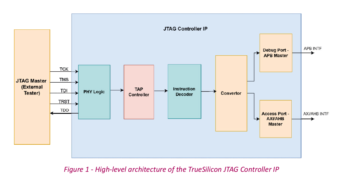
Figure 1 illustrates the high-level architecture of the TrueSilicon JTAG Controller IP, including the JTAG master, PHY logic for TCK, TMS, TDI, TDO driver, TAP controller state machine as per 1149.1 version, instruction and data registers, Scan chain logic and address, data & control system interface.
With its scalable and modular design, the TrueSilicon JTAG Controller IP provides a robust solution for manufacturing test, in-system debug, and post-silicon validation, significantly improving observability and controllability of SoC designs.